
TRW Space and electronics group
About the photo
This photo is from a Star Trek episode called Operation Annihilate! which air on April 13 1967 and was filmed on the TRW One Space Park campus in Redondo Beach CA. I believe this particular scene was shot at the north side of Building S. I worked in Building R6 about 10 minutes walk from here.
Originally named Thompson Ramo and Wooldridge Inc after a merger in 1958, it was later shortened to TRW. The company was mostly known for aerospace, automotive, and credit reporting and was listed 57th on the Fortune 500 list in 1986. TRW was acquired by Northrop Grumman Corporation in 2002 and is a reminder that all good things eventually come to an end.
My involvement
I worked for TRW from 1989 to 1998 where I supported several ground terminal projects. I continued to work sporadically as a contractor performing onsite digital receiver alignment and testing along, with some remote design assignments. I have lots of fond memories, and in hindsight, the best company that I've worked for. One never knows these things until later, but I have no regrets for the path life has laid out for me.
Engineering activities
VXI Clock Recovery Module
Chairman's Award for Innovation
Chairman's Award for Innovation
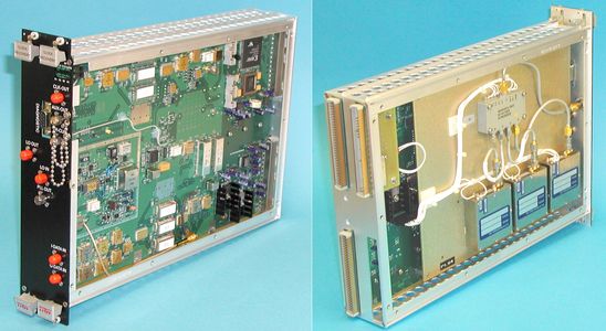
2001 contract - Photo of Clock Recovery Module front and rear without covers. As a contractor, I received this interesting design task to update and repackage their existing clock recovery design into this VXI form factor to support their new ground station receiver product line. The module supported 4 symbol rates with the last slot unused. The design supported multiple modulation formats with stringent phase noise and Eb/No acquisition requirements. Fortunately, I had the assistance of a board layout person along with a mechanical engineer for packaging (D. Kubo, et al).
Chairman's Award for Innovation
Chairman's Award for Innovation
Chairman's Award for Innovation
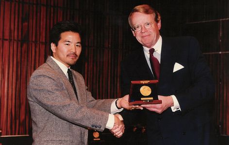
1998 - I was one of several recipients for the 1998 Chairman's Award for Innovation. This photo is of a much younger me at the TRW headquarters in Cleveland Ohio with then CEO Joe Gorman. They treated us quite well and it was a memorable occasion.
The innovation was the application of using raw subsampled demodulated data to steer the convergence algorithm of our suite of ground terminal instruments that included a cross polarization canceller and adaptive equalizer.